
Piezoelectric Generator
Sarah Qadar - PHYS 420 (2023-24)
Purpose
The purpose of designing this PCB (printed circuit board) was to demonstrate the feasibility of the use of piezoelectricity for sustainable power generation. This project explores relevance of piezoelectric materials to the future of wearable electronics and other devices powered by mundane human activities (ie. walking).
What is Piezoelectricity?

Conservation of Energy
“Energy can neither be created nor destroyed, only converted from one form to another”
Piezoelectricity is an example of the Law of Conservation of Energy!
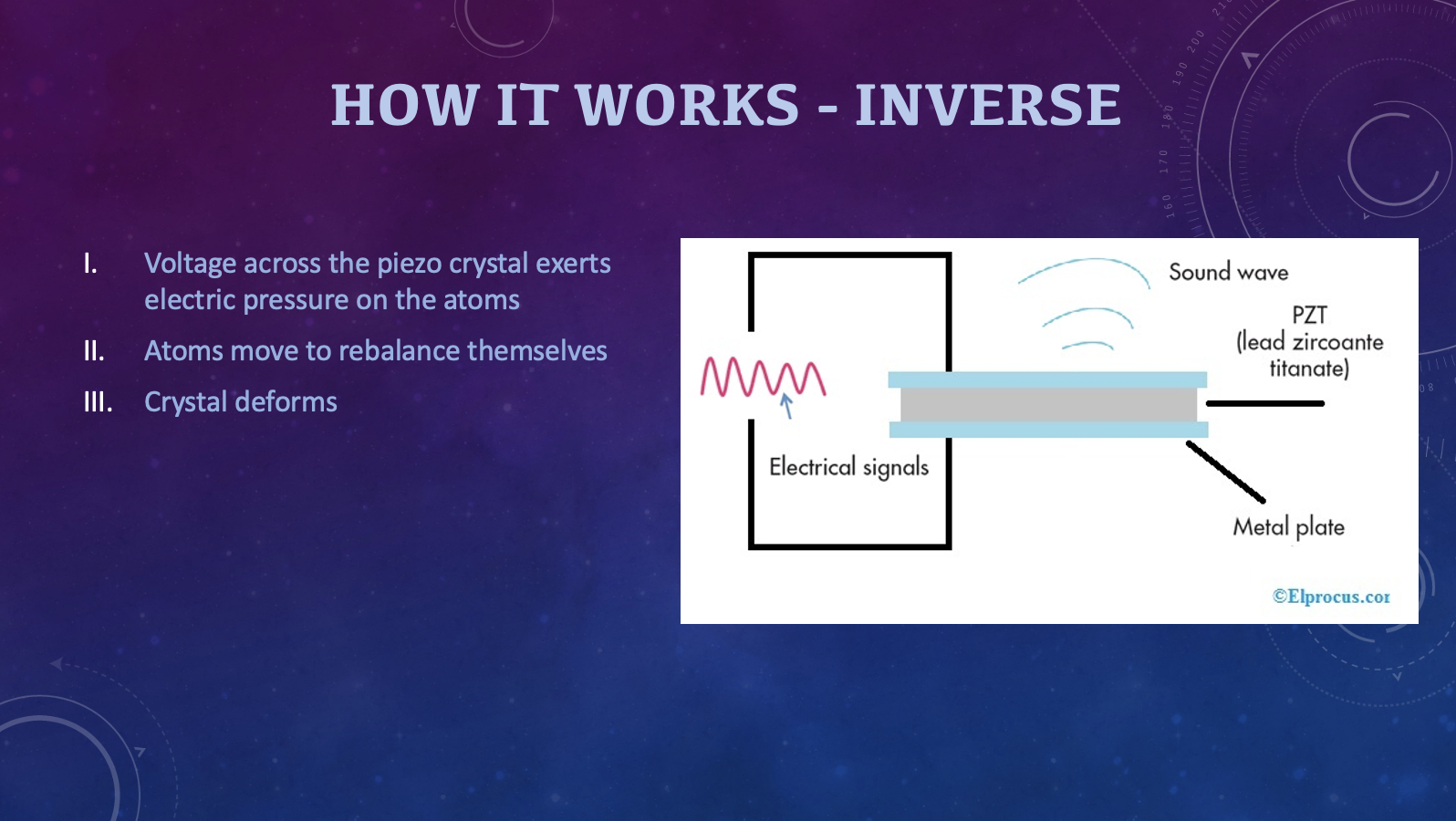
Inverse Piezoelectric Effect: Electrical energy converted into kinetic energy
Piezoelectric Materials
- Naturally occurring piezoelectric materials: quartz, topaz, tourmaline
- Structure mimicked to created synthetic materials (ex. PZT ceramic) to exhibit piezoelectric properties
- Crystalline structures of piezoelectric materials are NOT symmetrical
- Electrically neutral when unstressed due to balanced electric charges (cancel each other out)
- No charge build up on crystal faces
How Does it Work?

Applications of Piezoelectricity


Power Generation
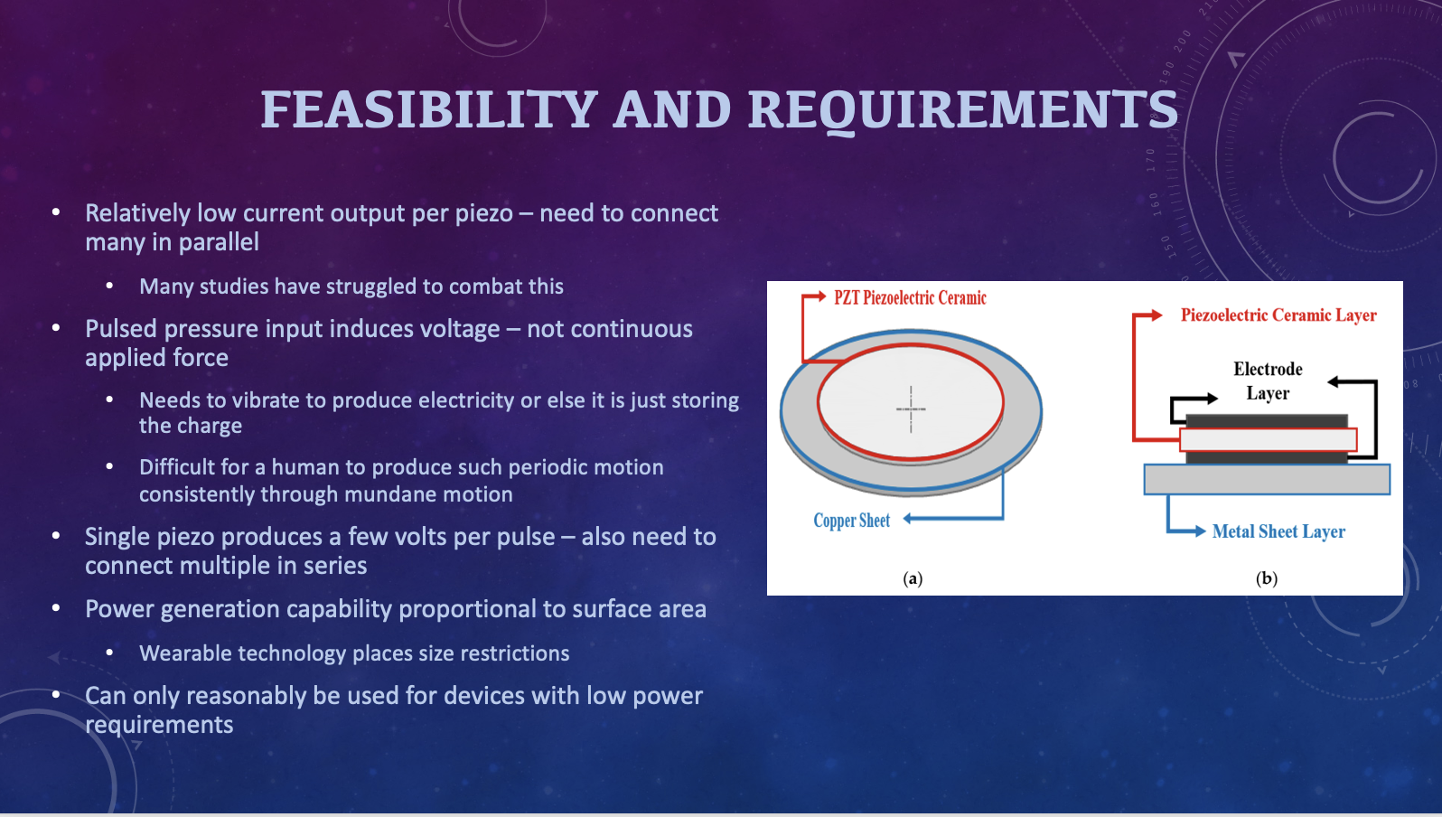
Due to the direct piezoelectric effect, piezo materials can act as mini power supplies! Optimizing piezoelectric systems to produce useable amounts of energy has been a focus of the growing field of microelectromechanics.

Demonstration Design
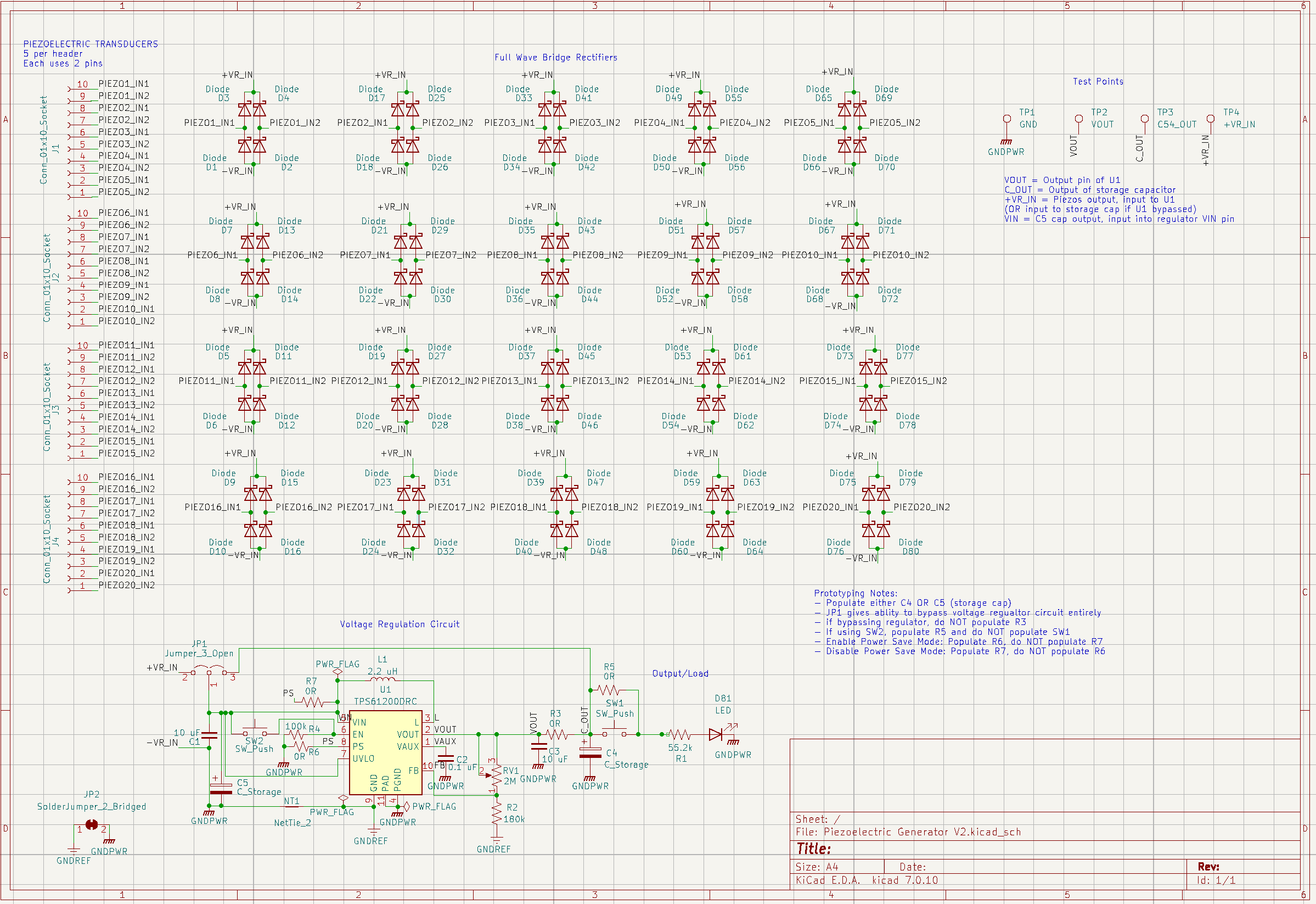
Schematic
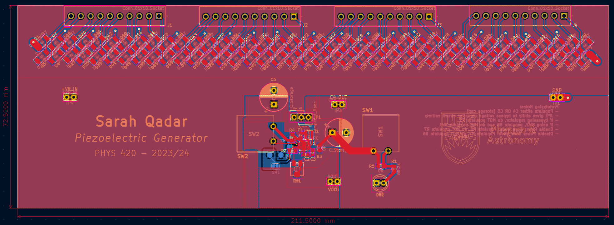
Layout
Front Copper Layer
Note: Length and width dimensions shown (mm). Front and back copper layers on.
Back Copper Layer

Note: Dimensions NOT shown. Front copper layer turned off.
PCB Bill of Materials
| RefDes | Item | Manu P/N | Footprint | Qty |
| N/A | Piezo Elements (with wire leads) | HD-PAB2701-2 | N/A | 1-20 |
| U1 | Voltage Regulator | TPS61202DRCR | 10VSON | 1 |
| C1, C3 | 10uF X7R OR X5R Capacitor | GRM188Z71A106KA73 | 0603 | 2 |
| C2 | 0.1uF X7R OR X5R Capacitor | C0603C104M5RAC7867 | 0603 | 1 |
| RV1 | max 2Mohm potentiometer | 3314J-1-205E | SMT J-LEAD | 1 |
| R1 | 55.2kohm resistor | ERJ-6GEYJ563V | 0805 | 1 |
| R2 | 180kohm resistor | ERA-6AEB184V | 0805 | 1 |
| J1-J4 | 10 position screw terminal | 1-1776275-0 | 3.5mm pitch | 4 |
| D1-D80 | Fast recovery diode | ES2BFSH | SOD-128 | 80 |
| D81 | Green diffused LED (3.2V) | QBL7IG60D | THT 5mm radial | 1 |
| R3, R4, R5 | 0 ohm resistor | RMCF0805ZT0R00 | 0805 | 3 |
| R6 | 100kohm resistor | ERA-6AEB104V | 0805 | 1 |
| JP1 | 3 position vertical header | TS-103-T-A | 2.54mm pitch, vertical, 3 position | 1 |
| JP1 | Jumper Cap | STC02SYAN | 2.54mm pitch, 2 position 2 | 1 |
| L1 | 2.2uH Inductor | LQH3NPH2R2MMEL | nonstandard | 1 |
| SW2 | pushbutton | GPTS203211B | nonstandard | 1 |
| C5 | 1000uF capacitor | 108CKE063M | THT, radial, 5mm pitch, 10mm diameter | 1 |
Assembly
Materials:
- PCB and its stencil
- Components listed in PCB bill of materials (see previous section)
- Solder paste (Sn63/Pb37 is my preferred)
- Tweezers, small Phillips screwdriver
- Reflow oven OR precision heat gun
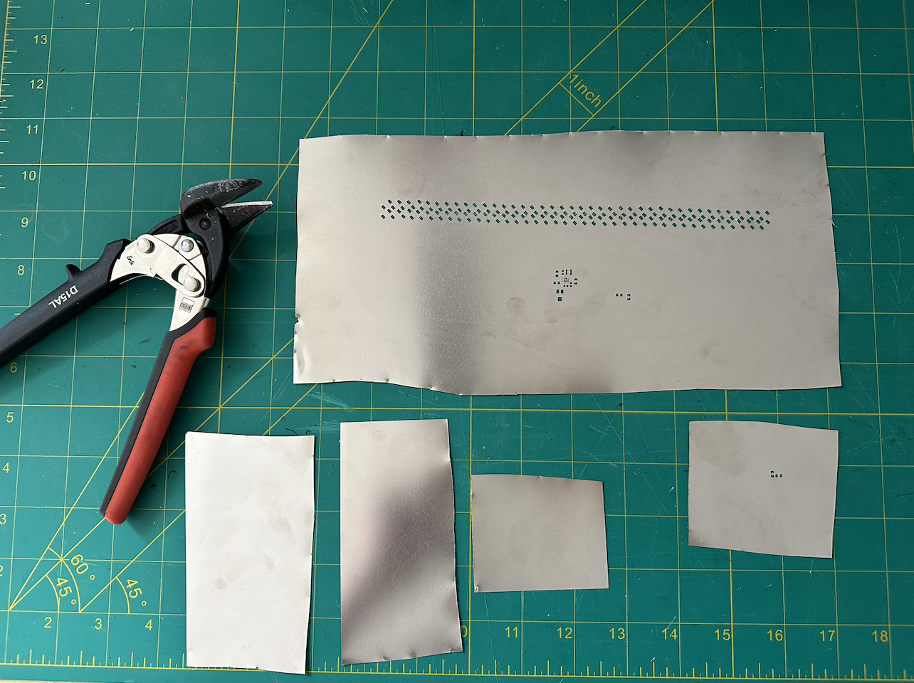
- Sheet metal scissors
- Soldering iron, solder spool—may also need flux, solder wick, solder sucker
- Masking tape, kapton tape, electrical tape
- Rubber sheet
Instructions:
- Use sheet metal scissors (left in below image) to cut the front and back stencils into two separate pieces as seen in the below image.
- Also cut out some squares and/or rectangles from the remaining sheet metal
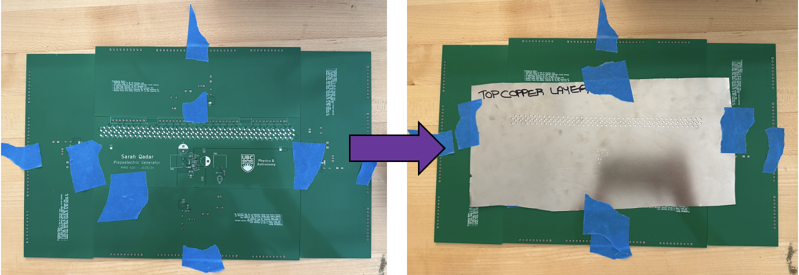
- When you order a PCB, it usually comes with 5 copies. Arrange and tape down (with masking tape) the other copies around the one you’re soldering to stabilize it.
- Place the stencil cutout of the side you're soldering onto the board, aligning the stencil with the footprints before taping it down with masking tape as well.
- Use one of the small sheet metal squares or rectangles to scoop solder paste out of the container and put it onto the stencil, roughly smearing it across all the footprints using the side of the metal piece.
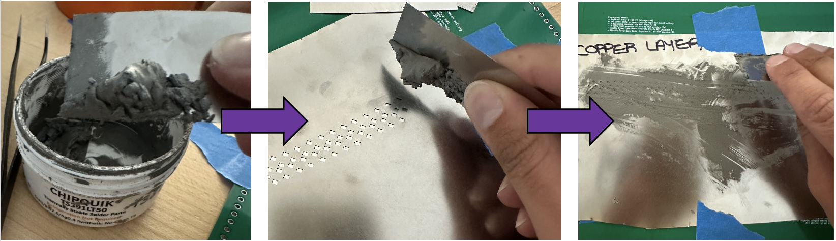
- Use the edge of the metal piece to scrape away the thick layer of solder paste, this will leave only the paste that was actually applied to each footprint while getting rid of the excess.
- Carefully remove the stencil, lifting upwards to avoid smudging the paste
- remember, It does not have to be perfect!
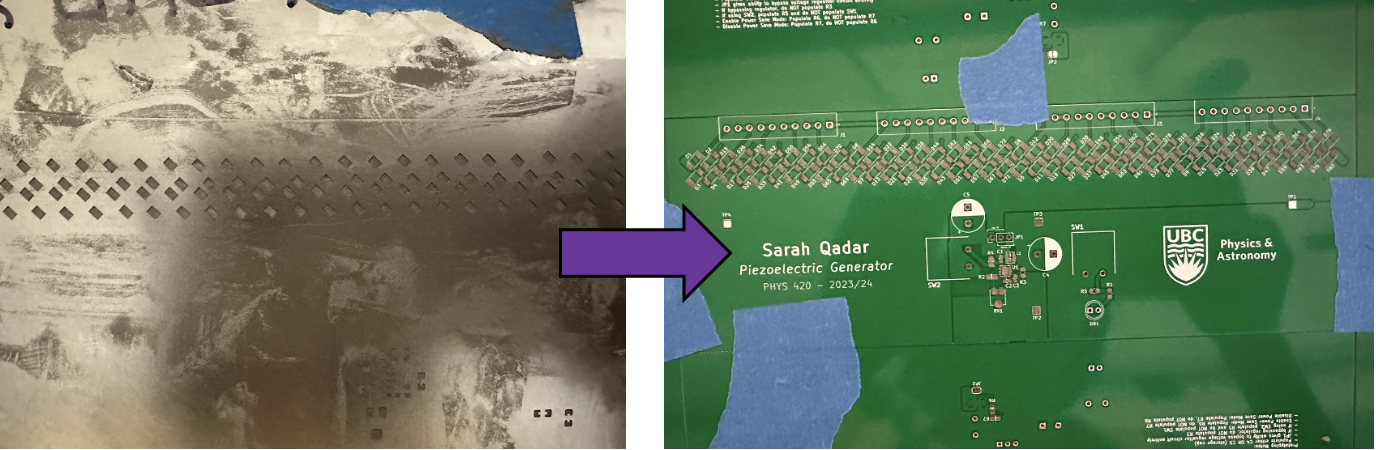
- Use the tweezers to place the components (see PCB bill of materials in earlier section) on their respective footprints (labeled with RefDes that can be cross referenced with the schematic and bill of materials).
- There are certain components that do NOT have to be populated for this particular demonstration.
- The PCB bill of materials ONLY includes what is needed to replicate my demonstration so don’t be alarmed when you see empty footprints.
- There are certain components that do NOT have to be populated for this particular demonstration.
- Reflow the solder paste either by placing the PCB into a reflow oven or by using a precision heat gun.
- Reflow Oven - Select a reflow waveform by matching up the wave in the solder pastes data sheet to one of the machines options.
- Precision heat gun - Don’t aim the heat gun at any particular component for too long, just long enough that the solder melts, becoming shiny.
- For the components on the back, you can either hand solder them on or repeat steps 3-7 with the back stencil.
- If you choose to use the reflow oven again, cover the components on the front of the board with kapton tape to protect them.
- It would be most convenient to just use the heat gun for the components on the back since there are so few.
- If you choose to use the reflow oven again, cover the components on the front of the board with kapton tape to protect them.
- Now hand solder the through hole components then insert the piezo leads into the screw terminals, using the small Phillips screwdriver to secure them in.
- Insert the jumper cap on the 2 pins of JP1 that are labeled “Use VR”.
- Use the sheet metal scissors to cut circles the size of the inner circles on your piezo elements out of the rubber sheet then use duct tape or electrical tape to stick them onto the aforementioned inner circles.
- Don’t place the tape across the element. Fold the piece of tape over such that the sticky part is double sided and stick that directly on the piezos inner circle to which you can press the rubber circle onto.
- Don’t place the tape across the element. Fold the piece of tape over such that the sticky part is double sided and stick that directly on the piezos inner circle to which you can press the rubber circle onto.
- Stack the piezo elements into some sort of rigid holder (tall enough to fit all).
- Make sure you have a narrow enough cylindrical item to repeatedly tap the piezo stack with later (even the back of the screwdriver would work for this).
Demonstration
Materials:
- The PCB
- Multimeter (with regular probes and alligator clip leads)
- Oscilloscope (with clip probes)
- Extra piezo element (ie. NOT attached to the PCB)
3 Part Demo
Part 1
- Attach the oscilloscope probes clips to the extra piezo elements wire leads.
- Holding the piezo element down to a flat surface by its edge, rapidly tap on the inner circle.
You should see an AC signal (produced by your tapping) on the oscilloscope!
Part 2
To charge up a capacitor to store this energy we produced from tapping, the AC signals need to be converted to DC via the full wave bridge rectifiers.
- Put a multimeter with regular probes on the continuity setting then probe the leads of SW1 to ensure its NOT continuous (switch closed).
- Replace the multimeters regular probes with the alligator clip type and put it on the DC voltage setting.
- Attach the ground probe to the test point on the PCB labeled GND and attach the other to the test point labels +VIN.
- Use a narrow cylindrical item (like the back of a screwdriver) to rapidly tap the stack of piezos in the holder.
On the multimeter you will see the voltage gradually increase as you charge up the capacitor, demonstrating the harvesting of energy from piezoelectric elements!
Part 3
Now that we’ve generated and stored all this voltage, lets demonstrate that even in this small, rudimentary setup, piezo materials can be used to actually power things!
- Dim or turn off the lights and ensure the PCB is clearly visible to anyone in the room.
- Charge the capacitor up a bit while monitoring the increasing voltage then detach the multimeter clips from the test points.
- Click the button (SW1)
The green LED (D81) will briefly light up, powered by the electricity you generated by tapping the piezo elements!